Sample Shipments Begin for Our Low-Profile SWIR Flip-Chip LED
Marubeni America Corporation is pleased to announce that we will begin shipping samples of our “epitex F Series” LED chip, which operate in the SWIR range of 1050nm to 1900nm and feature a low-profile, compact design. The sample shipments are set to start in August 2024 (see Figure 1 and Table 1).
We are excited to share that this newly developed chip is a pioneering achievement, being the world’s first*1 to utilize a flip-chip structure with InP (Indium Phosphide) materials. This innovative design eliminates the need for current injection wires, significantly reducing the height required for chip mounting and enabling low-profile LED packaging. Additionally, the absence of wire bonding space on the package side allows for high-density mounting, especially when multiple LED chips are arranged together, making the miniaturization of the package much simpler. The wireless design also removes any shadow effect caused by wires on the light-emitting surface, making optical design more straightforward (see Figure 2).
In terms of performance, the absence of electrodes on the light extraction surface enhances light extraction efficiency. Despite its small size of 270μm × 170μm, the chip achieves the same light output as the existing high-brightness SWIR LED “epitex D Series” chip, which measures 320μm × 320μm.
Given these outstanding characteristics and the capability for low-profile, compact packaging, this product is expected to significantly contribute to applications where device footprint is limited, such as in smartphones and other small electronic devices, vital sensing, and proximity sensors.
*1 According to our partner manufacturer’s research
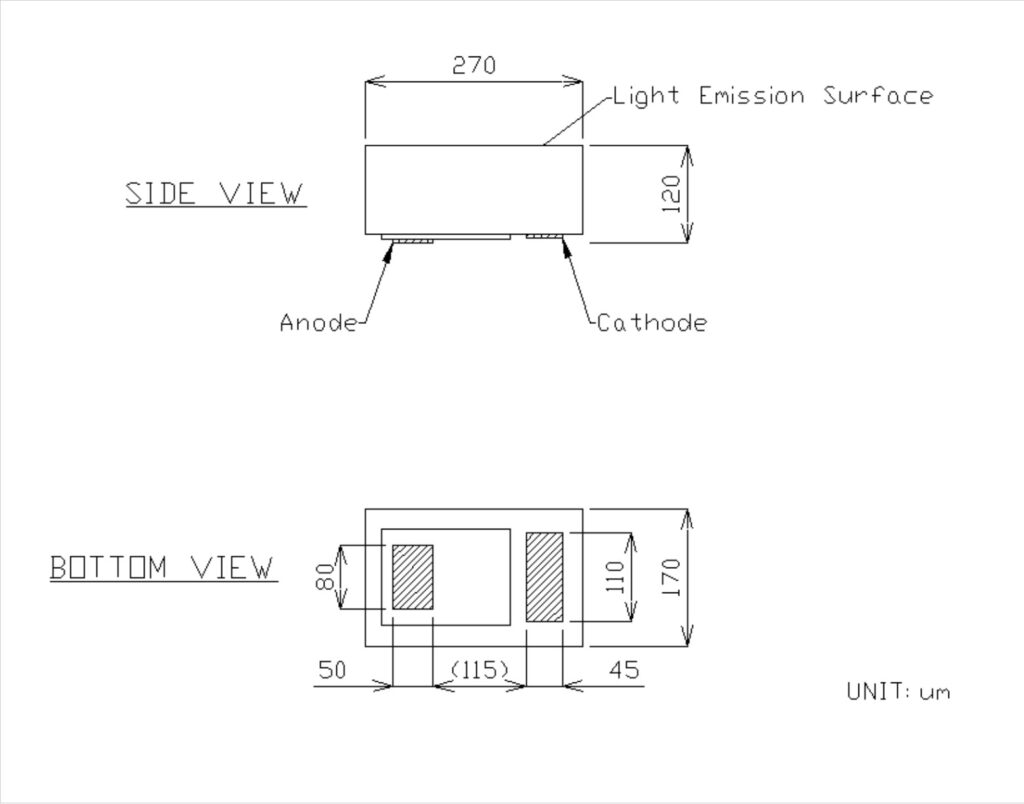
Figure 1
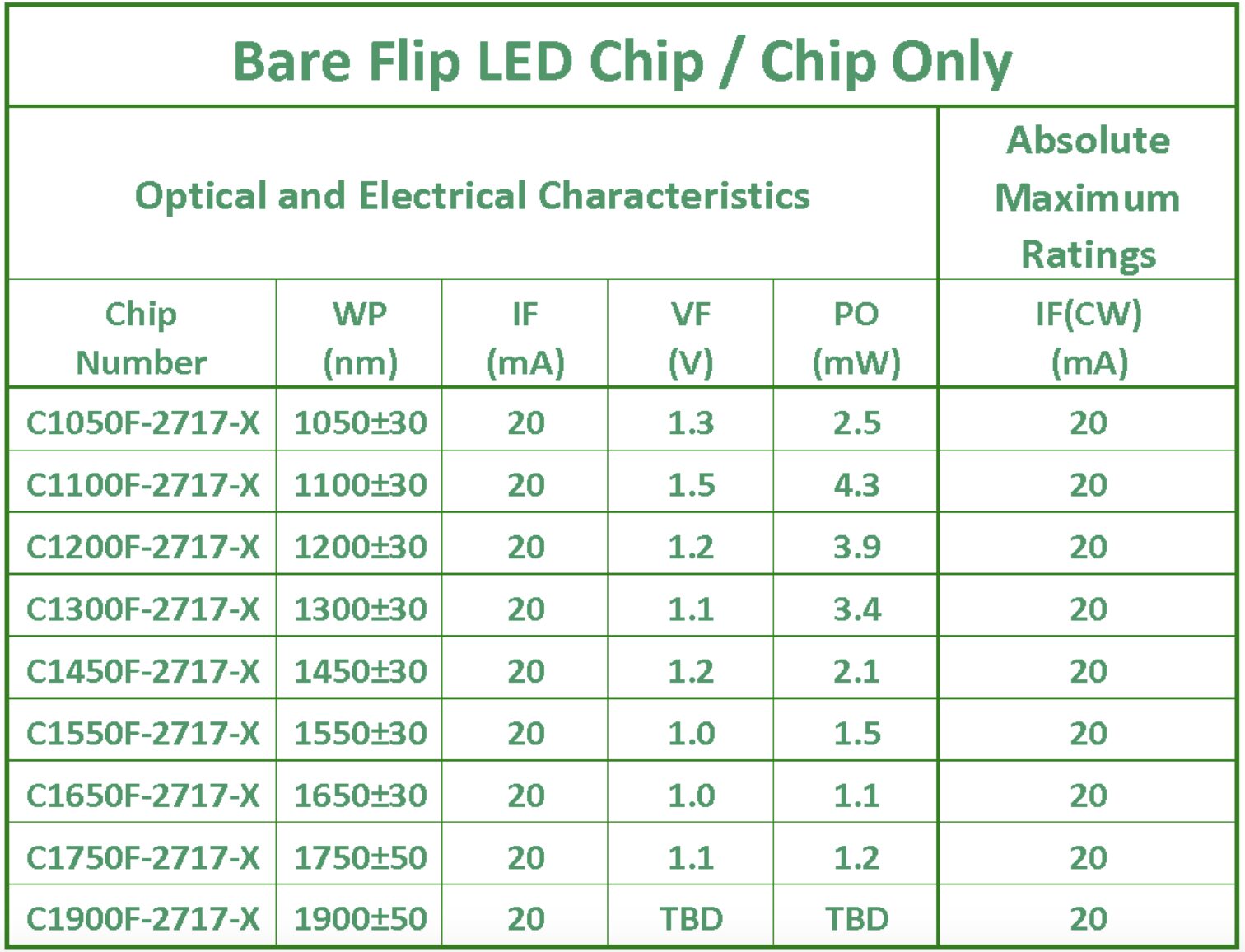
Table 1
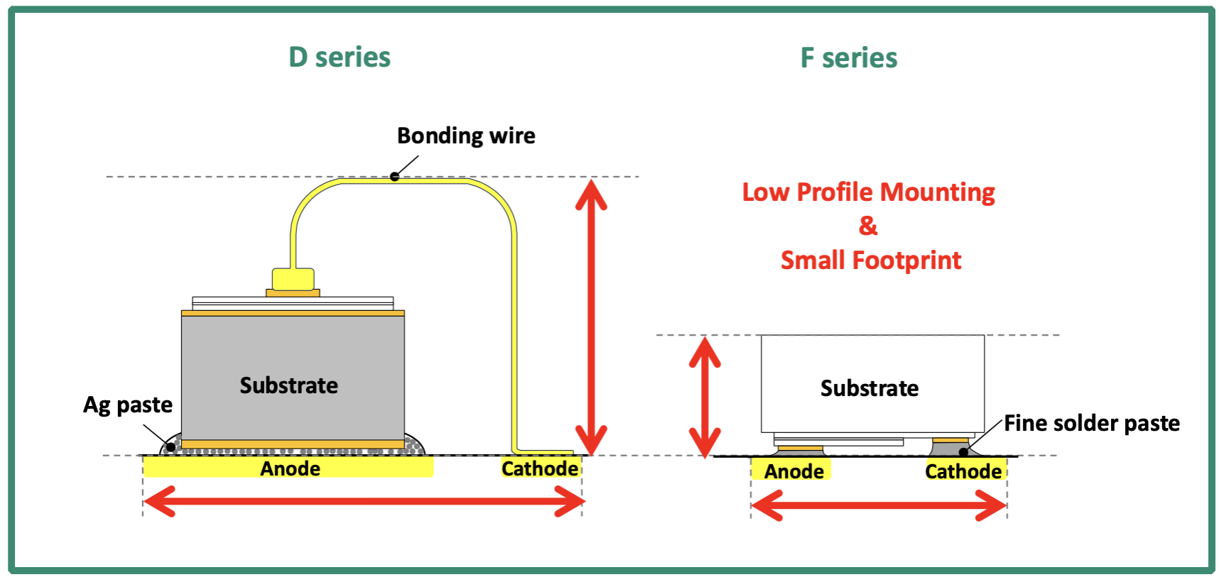
Figure 2
Datasheets
- C1050F-2717-X
- C1100F-2717-X
- C1200F-2717-X
- C1300F-2717-X
- C1450F-2717-X
- C1550F-2717-X
- C1650F-2717-X
- C1750F-2717-X
Main Applications
- Light Source for Biosensing
- Vital Sensing Light Source for Mobile Devices
Contribution to the Biosensing Field
We believe that the flip-chip in the SWIR wavelength range will also make valuable contributions to the biosensing field. The SWIR region includes the “second biological window*2” at 1100-1350nm and the “third biological window*2” at 1550-1800nm, where the penetration depth into biological tissues is longer. This allows light to reach deep inside tissues non-invasively, providing more accurate information for evaluating fine structures and lesions within biological tissues (see Figure 3). Furthermore, the SWIR region contains absorption bands for many substances such as water, glucose, ethanol, and cholesterol. By detecting and accurately quantifying these substances through the transmittance and absorption rates of SWIR light, it becomes easier to monitor important biological indicators. This advancement is expected to significantly benefit research in the biosensing field and improve the accuracy of non-invasive biological diagnostics.
Moreover, since the flip-chip does not require wires for current injection, it can be mounted on flexible substrates. Flexible substrates are lightweight and can be freely bent and placed within electronic devices, making it easier to reduce the weight and size of electronic devices (see Figure 4). This is expected to contribute to the miniaturization of mobile devices and medical sensing equipment that continuously monitor vital signs.
*2 Infrared light with wavelengths of approximately 700-2500nm is less scattered and absorbed by molecular vibrations in biological tissues, making it suitable for deep tissue observation and sensing. This wavelength range is referred to as the “biological window.”
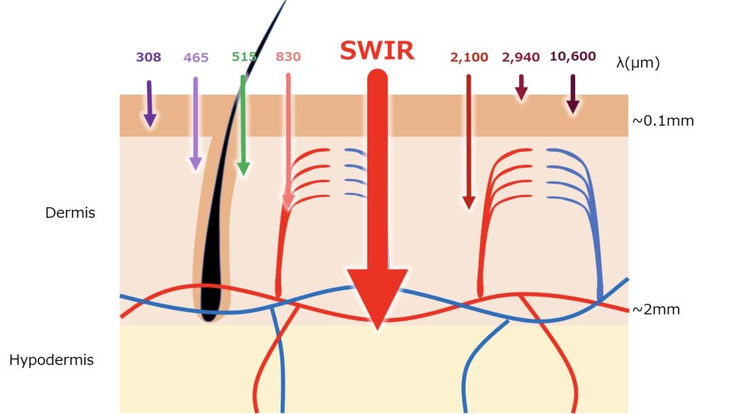
Figure 3
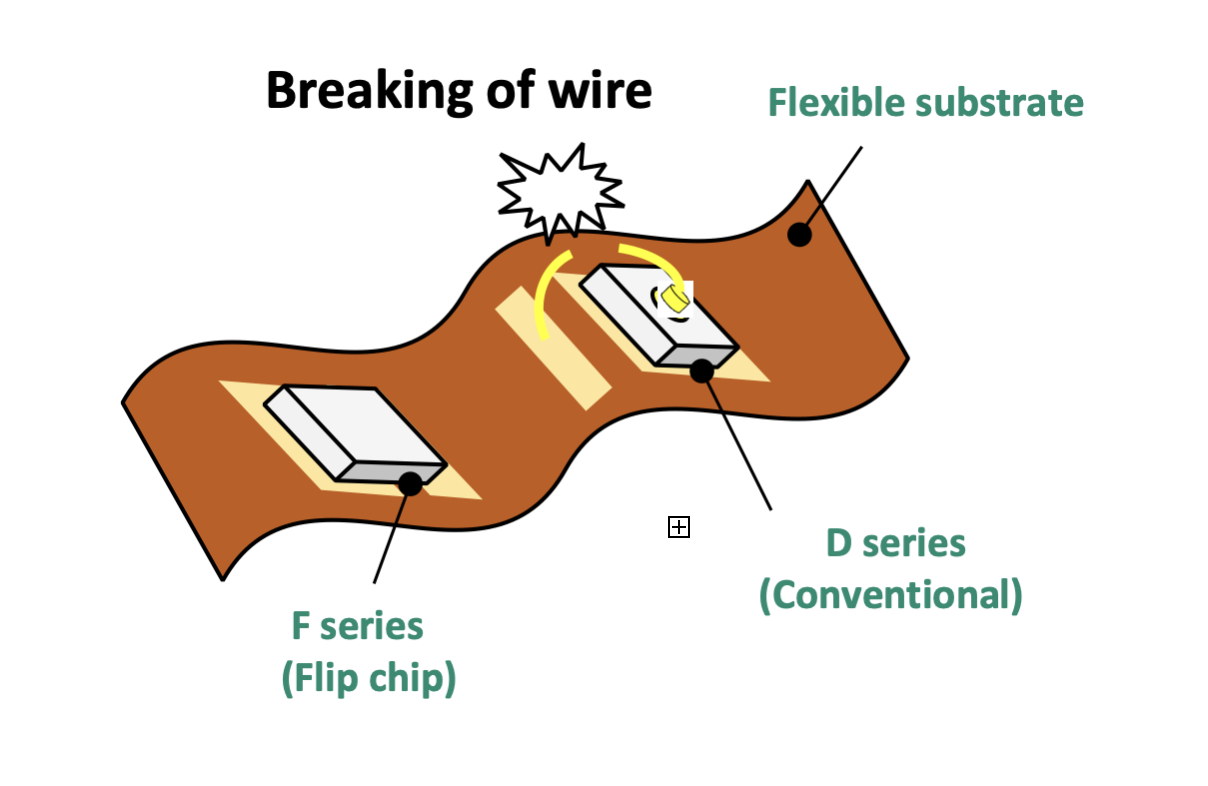
Figure 4
Chip Mounting Method
The developed chip has a height difference between the anode and cathode electrodes, and the electrode dimensions are small. Therefore, it is recommended to use fine solder with a particle size of approximately 20μm or less for mounting.
About the Ultra-Compact Package with Flip-Chip
We plan to start shipping test samples of the ultra-compact package with the developed “epitex F Series” LED chip in the SWIR wavelength range (package size is expected to be 1.0mm or less) in October 2024. Please contact us if you are interested in requesting samples.