New developed product announcement
An Ultra-compact SWIR LED Package with a Footprint of 0.6 x 0.3 mm
Adopts the world’s first SWIR LED chip utilizing a flip-chip structure with InP materials*1
Marubeni America Corporation (hereinafter “MAC”) is pleased to announce that it has developed an ultra-compact LED package with a footprint of 0.6 x 0.3 mm (“EDP package”) that operates in the wavelength range of 1050 to 1650 nm, which is the SWIR region, and will begin shipping test samples within Japan and overseas from November 2024.
The wavelengths in the SWIR region are suitable for applications such as smartphones and other small electronic devices, vital sensing, and proximity sensors, and for non-invasive deep measurement and imaging using the “second biological window” at 1100 to 1350 nm and the “third biological window” at 1550 to 1800 nm*2. However, due to limitations in device footprint, there is demand for even smaller LED packages.
To meet this demand, our manufacturer partner adopted the world’s first LED chip utilizing a flip-chip structure with indium phosphide (InP) materials, eliminating the need to provide space for wire bonding on the package side and thus achieving a significant reduction in package size. In addition, the wireless design removes any shadow effect caused by wires on the light-emitting surface, improving the output power and illuminance distribution.
Moreover, since this product is an LED package with the chip protected by transparent resin, solder mounting is easier compared to bare chips. Additionally, it has a footprint equivalent to the 0603 size (0.6 × 0.3mm) of small electronic components such as chip resistors, allowing it to be handled in the same way as 0603-sized electronic components during mounting on substrates.
As a result, this product is expected to contribute not only to applications where device footprint is limited, such as smartphones and other small electronic devices, vital sensing, and proximity sensors, but also to the advancement of research in the biosensing field and improvement in the accuracy of non-invasive biological diagnostics.
We will continue to support technological innovation in society by developing more advanced LEDs and LED packages in the future.
By molecular vibrations in biological tissues, making it suitable for deep tissue observation and sensing. This wavelength range is referred to as the “biological window.”

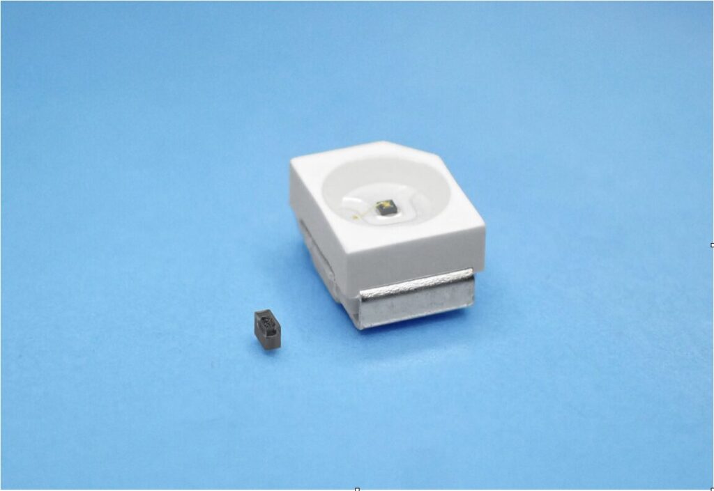
Comparison with previous Ushio product (this product is on the left)
Main Applications
- Sensing light source for mobile devices
- Light source for biosensing
Parts Numbering
The name of this package is EDP.
When making inquiries, please mention EDP for a smoother process.
The model number is subject to change during mass production. Thank you for your understanding.
Example: EDP1200F-1027-X
(a) (b) (c) (d) (e) (f)
(a)EDP: Package Family Name
(b)1200: Peak Wavelength.
(c):F: Structure Type of LED Chips (Unelectable Option)
(d)1: Number of Chips (1: 1 Chip)
(e)027: LED Chip Dimension (027: 270μm*170μm)
(f) -X : Prototype (Not included after mass production)
Reference material
Contribution to the Biosensing Field
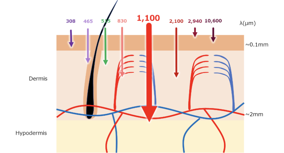
The SWIR region includes the “second biological window” at 1100 to 1350 nm and the “third biological window” at 1550 to 1800 nm. Since penetration into biological tissues is deeper, these windows allow light to reach deep inside biological tissues non-invasively, making them suitable for non-invasive deep measurements and imaging, and leveraging this characteristic enables more accurate information to be provided for evaluating fine structures and lesions within biological tissues (see Figure 1).

Figure 1
Furthermore, the SWIR region contains absorption bands for many substances such as water, glucose, ethanol, and cholesterol. By detecting and accurately quantifying these substances through the transmittance and absorption rates of SWIR light, it becomes easier to monitor important biological indicators, and this is expected to contribute to the advancement of research in the biosensing field and improvement in the accuracy of non-invasive biological diagnostics.
*1 According to research conducted by our manufacturing and design partner (USHIO INC.)
*2 Infrared light with wavelengths of approximately 700 to 2500 nm is less scattered and absorbed