Ultra-Compact: EDP
An Ultra-compact SWIR LED Package with a Footprint of 0.6 x 0.3 mm
Adopts the world’s first SWIR LED chip utilizing a flip-chip structure with InP materials*1
Marubeni America Corporation (hereinafter “MAC”) is pleased to announce that it has developed an ultra-compact LED package with a footprint of 0.6 x 0.3 mm (“EDP package”) that operates in the wavelength range of 1050 to 1650 nm, which is the SWIR region, and will begin shipping test samples within Japan and overseas from November 2024.
The wavelengths in the SWIR region are suitable for applications such as smartphones and other small electronic devices, vital sensing, and proximity sensors, and for non-invasive deep measurement and imaging using the “second biological window” at 1100 to 1350 nm and the “third biological window” at 1550 to 1800 nm*2. However, due to limitations in device footprint, there is demand for even smaller LED packages.
To meet this demand, our manufacturer partner adopted the world’s first LED chip utilizing a flip-chip structure with indium phosphide (InP) materials, eliminating the need to provide space for wire bonding on the package side and thus achieving a significant reduction in package size. In addition, the wireless design removes any shadow effect caused by wires on the light-emitting surface, improving the output power and illuminance distribution.
Moreover, since this product is an LED package with the chip protected by transparent resin, solder mounting is easier compared to bare chips. Additionally, it has a footprint equivalent to the 0603 size (0.6 × 0.3mm) of small electronic components such as chip resistors, allowing it to be handled in the same way as 0603-sized electronic components during mounting on substrates.
As a result, this product is expected to contribute not only to applications where device footprint is limited, such as smartphones and other small electronic devices, vital sensing, and proximity sensors, but also to the advancement of research in the biosensing field and improvement in the accuracy of non-invasive biological diagnostics.
We will continue to support technological innovation in society by developing more advanced LEDs and LED packages in the future.
By molecular vibrations in biological tissues, making it suitable for deep tissue observation and sensing. This wavelength range is referred to as the “biological window.”
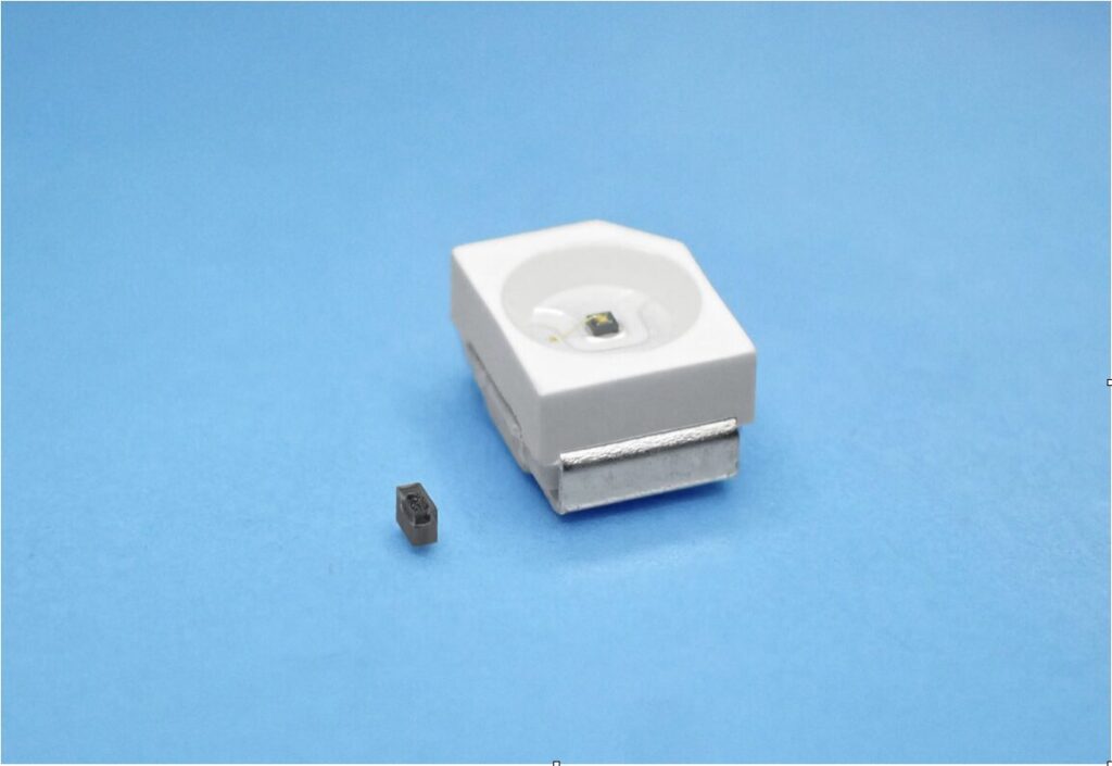
Comparison with previous Ushio product (this product is on the left)
Main Applications
- Sensing light source for mobile devices
- Light source for biosensing
Parts Numbering
The name of this package is EDP.
When making inquiries, please mention EDP for a smoother process.
The model number is subject to change during mass production. Thank you for your understanding.
Example: EDP1200F-1027-X
(a) (b) (c) (d) (e) (f)
(a)EDP: Package Family Name
(b)1200: Peak Wavelength.
(c):F: Structure Type of LED Chips (Unelectable Option)
(d)1: Number of Chips (1: 1 Chip)
(e)027: LED Chip Dimension (027: 270μm*170μm)
(f) -X : Prototype (Not included after mass production)
Reference material
Contribution to the Biosensing Field
The SWIR region includes the “second biological window” at 1100 to 1350 nm and the “third biological window” at 1550 to 1800 nm. Since penetration into biological tissues is deeper, these windows allow light to reach deep inside biological tissues non-invasively, making them suitable for non-invasive deep measurements and imaging, and leveraging this characteristic enables more accurate information to be provided for evaluating fine structures and lesions within biological tissues (see Figure 1).
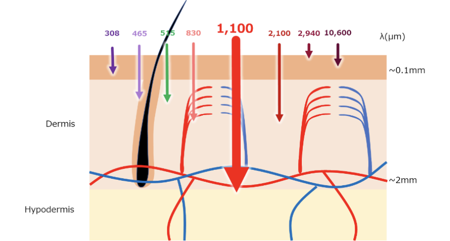
Figure 1
Furthermore, the SWIR region contains absorption bands for many substances such as water, glucose, ethanol, and cholesterol. By detecting and accurately quantifying these substances through the transmittance and absorption rates of SWIR light, it becomes easier to monitor important biological indicators, and this is expected to contribute to the advancement of research in the biosensing field and improvement in the accuracy of non-invasive biological diagnostics.
*1 According to research conducted by our manufacturing and design partner (USHIO INC.)
*2 Infrared light with wavelengths of approximately 700 to 2500 nm is less scattered and absorbed
Loading...
Loading...
EDP Series
The EDP series represents Tech-LED’s ultra-compact LED chips in packaged form, pushing miniaturization to the limit for high-tech applications. EDP devices are essentially bare LED dies with minimal encapsulation, resulting in packages as small as 0.6 mm × 0.3 mm – truly microscopic dimensions. (In fact, 0.6 × 0.3 mm corresponds to the 0201 footprint in inch units.) These are among the smallest packaged LEDs available on the market. The EDP series was developed to serve emerging needs in microelectronics, such as micro-LED displays, optical sensors with tight space constraints, and any application where dozens or hundreds of tiny LEDs might be arrayed together. Despite their size, EDP LEDs are available in specialty wavelengths including SWIR, as well as standard colors, making them a powerful tool for designers looking to integrate light sources at a microscale.
Features of the EDP Ultra-Compact Series
- Minuscule Footprint (0201-Class): EDP LEDs are extraordinarily small – comparable to a grain of sand. With a package area roughly 0.18 mm² (0.6 mm by 0.3 mm), they consume negligible board space. This size category allows placement of light emitters in high-density grids or in tiny cavities where no other light source would fit. For perspective, you could fit several EDP LEDs on the head of a pin. Their low profile also means they sit almost flush with the PCB, which is advantageous for applications like micro-displays or tightly stacked electronics. This ultra-compact packaging is achieved through advanced processes where the LED die itself forms the structural and electrical basis of the “package” – similar to chip-scale, but EDP may even forego a traditional substrate in favor of direct solderable contacts on the die.
- Optimized for Arrays and Matrix Assemblies: The EDP series is typically used when many LEDs are needed in proximity. As such, we supply these LEDs in formats conducive to array assembly (for example, on tape in ultra-fine pitch or in wafer-level form). They can be placed with standard SMT equipment configured for small chip placement. Once on the PCB or substrate, their tiny size enables pixel pitches of under 1 mm easily – crucial for micro-LED displays or high-resolution sensing arrays. Designers can create LED matrices with EDP parts that approach the density one would get with unpackaged dies, but with the convenience of a packaged component. Whether you need a 10×10 array of LEDs for a mini matrix or thousands for a display, EDP makes it feasible without manual die bonding.
- SWIR and Special Wavelength Capability: One of the differentiators of Tech-LED’s EDP line is that it includes not just visible micro-LEDs but also short-wave infrared (SWIR) micro-LED chips. Historically, SWIR LEDs (like 1300–1600 nm) were limited to larger packages due to low efficiency and the need for heat dissipation. However, we have transferred our SWIR technology into the EDP format, meaning you can get, for instance, a 1350 nm or 1550 nm LED chip in an ultra-compact form. This is valuable for SWIR imaging and sensing arrays (e.g., a SWIR LED matrix for scene illumination in a multi-spectral imager). It aligns with our offerings of InGaAsP SWIR LED chips at the wafer level. Now, those chips are available in tiny solderable packages. On the visible side, EDP covers from UV through NIR too – so an engineer could mix UV, visible, and SWIR EDP LEDs side by side in a very small optical module for broad spectral coverage.
- Ideal for Micro-LED Displays and Indicators: EDP is at the core of micro-LED display innovation. For AR glasses or HUDs requiring micro-projection, having micro-LEDs as pixels (with each LED possibly in the tens of microns) is desired for brightness and efficiency. Our EDP chips serve as those pixels. Because they are pre-packaged, integrating them can be easier than raw dies. They can be directly bonded onto a driver circuit substrate in a matrix form. High-resolution LED arrays on the order of 1000+ PPI (pixels per inch) are achievable with EDP class LEDs. Additionally, in more conventional electronics, an EDP LED can act as a micro indicator – for example, a tiny status light on a very small device or PCB, where even a 1.6 mm (0603) LED is too large. With minimal power, an EDP LED can still emit a visible spot of light, sufficient for an indicator, while occupying essentially no board real estate.
- Customization for Sensing Integration: EDP LEDs can also be integrated directly into sensor packages or MEMS devices due to their size. We can provide them in formats that allow mounting into custom cavities or on unusual substrates. For instance, an array of EDP IR LEDs could be integrated on the same silicon die as photodetectors to create a lab-on-chip that emits and detects light in micro channels – achieving a fully integrated optical sensor. The small size and low thermal output (when pulsed or low current) ensure they don’t perturb their environment much. In short, EDP LEDs enable a level of integration between light emitters and semiconductor sensors that was impractical before. A concrete example: a company developing a micro-spectrometer could embed multiple EDP LEDs of different wavelengths around a photodiode array to create an on-chip multi-wavelength illuminator for analyzing a sample, all within a few millimeters.
Applications of EDP Ultra-Mini LEDs
The potential applications for EDP series LEDs span cutting-edge tech sectors. One primary area is micro-LED displays and micro-projection. In AR smart glasses, micro projectors based on micro-LED matrices are emerging; our EDP (and EDCC) technology provides the micro emitters for these systems. If a display needs a full-color pixel that’s 10–20 microns wide, we can achieve that by combining micro-EDP UV chips with color converters or using trio of micro LEDs (red, green, blue) each of similar size. The high brightness possible from EDP LEDs ensures these micro displays can be bright enough for augmented reality under daylight.
Another area is optogenetics and biomedical implants. EDP LEDs are so small that they can be attached to neural probes or even injected (encapsulated appropriately) into living tissue to deliver light at a cellular level. Researchers in optogenetics need tiny light sources to activate neurons via light-sensitive channels; an EDP blue LED attached to a fine probe can target a specific brain region without affecting surrounding areas. Its small size minimizes tissue damage upon insertion. Similarly, EDP IR LEDs could be implanted superficially for continuous glucose monitoring or other in-vivo sensing, emitting light through skin to interact with biochemical markers, with minimal invasiveness.
Fiber-optic communications and sensors can also exploit EDP LEDs. For instance, creating a very compact optical transmitter: an EDP 1300 nm LED could be directly coupled to an optical fiber or integrated into a fiber connector for short-distance communication (like plastic optical fiber links) or sensing. A bundle of different EDP LEDs could feed a multi-fiber array for a spectroscopic sensor system, each fiber carrying a different wavelength to a remote probe (this approach could make a rugged multi-wavelength sensor head for chemical analysis, with the electronics safely at a distance). The minuscule size allows the source assembly to be extremely small or to fit many sources in a small space.
Consumer electronics will also find uses for EDP LEDs as tech trends push for smaller devices. Imagine future wearables the size of a coin – they might still need an LED for user feedback or for sensing (heart rate, SpO₂, etc.), and EDP provides that without consuming precious space. Even something like a backlit keyboard could one day use micro-LEDs per key for ultra-thin form factors, with EDP LEDs embedded in the key switches.
In summation, the EDP series opens possibilities where LEDs behave almost like integrated circuit components – tiny, array-ready, and able to be sprinkled across designs wherever light is needed but space is severely limited. Tech-LED supports these forward-looking applications by providing EDP LEDs in custom arrays or formats as required. We’re essentially giving product designers “drops of light” at the scale of electronics, empowering innovations in micro-displays, advanced biomedical devices, high-density optical sensors, and any application where conventional LEDs are just too large. When every fraction of a millimeter counts, the EDP series is the solution to bring illumination and sensing to the next level of miniaturization.