EDCC
Introducing the Compact High-Power LED EDCC Family Release
Marubeni America Corporation (hereafter referred to as MAC) is proud to announce the development of a new high-power LED package called the "EDCC Family," designed with a focus on compactness and high-density integration. Production of the EDCC Family is set to commence in the first quarter of 2024.
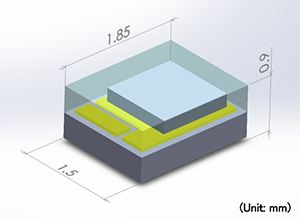
The EDCC Family incorporates traditional high-power LED chips with a wide range of wavelength options, yet it achieves an impressive reduction in footprint of approximately 80% when compared to the previous small-sized EDC Family package. As a result, it offers a compact form factor (W1.5 x L1.85 x H0.9 mm) that closely resembles bare chips and is also compatible with CSP (Chip Scale Package) and other compact-sized packages. This ensures not only ease of customization but also the convenience of handling SMD (Surface Mount Device) packages.
Key Features:
・Utilizes high-power LED chips with a wide wavelength range, including UV, visible light, IR, and SWIR, similar to those used in the SMBB Family and EDC Family.
・Compact-sized package, comparable to CSP and high-power LED chips, facilitating easy customization in an SMD-type LED format.
・Package design optimized for high-density integration.
Applications:
The EDCC Family is suitable for a wide range of applications that require high brightness, high output, and the combination of multiple wavelengths, including but not limited to:
- Machine Vision
- Optical Sorting
- Plant Growth
- Security
- Surveillance Cameras
- Optical Authentication
- Inspection Equipment
- Vital Sensing and more.
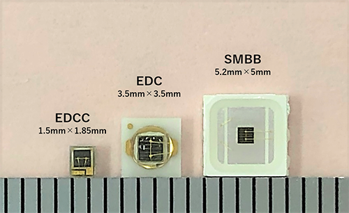
Comparison with conventional products
|
SMBB Flat |
EDC Flat |
EDCC |
|
|
Package area(mm) |
5.0×5.2 |
3.5×3.5 |
1.5×1.85 |
|
Appearance |
 |
 |
 |
Comparison
|
SMBB850DS-1100 |
EDC850DS-1100 |
EDCC850DS-1100 |
||
|
Vf[V]@1A |
3.2 |
3.2 |
3.2 |
|
|
Vfp[V]@5A* |
4.6 |
4.6 |
4.6 |
|
|
Po[W]@1A |
1.4 |
1.4 |
1.2 |
|
|
Po[W]@5A* |
5.6 |
5.6 |
5.3 |
|
|
Rthjs[K/W] |
9 |
11 |
21 |
|
|
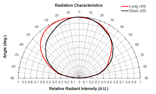
φ1/2[deg.] |
64 |
66 |
Long** |
69 |
|
Short** |
66 |
|||
*Pulse Condition: On Time 10us, Duty 1%
**Radiation Characteristics of EDCC Package

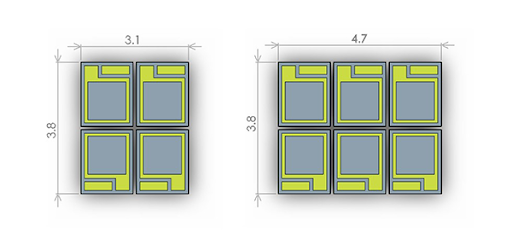
Package Design Optimized for High-Density Integration
The EDCC Family features a package design specifically tailored for high-density integration.
When EDCC packages are arranged in a 2 x 2 configuration, they fit within a compact 4mm x 3.2mm footprint, offering a package size nearly equivalent to the EDC package. Even when arranged in a 2 x 3 configuration, the total footprint remains compact at 4mm x 4.9mm, surpassing the SMBB package in terms of package area efficiency.
Example of LED placement
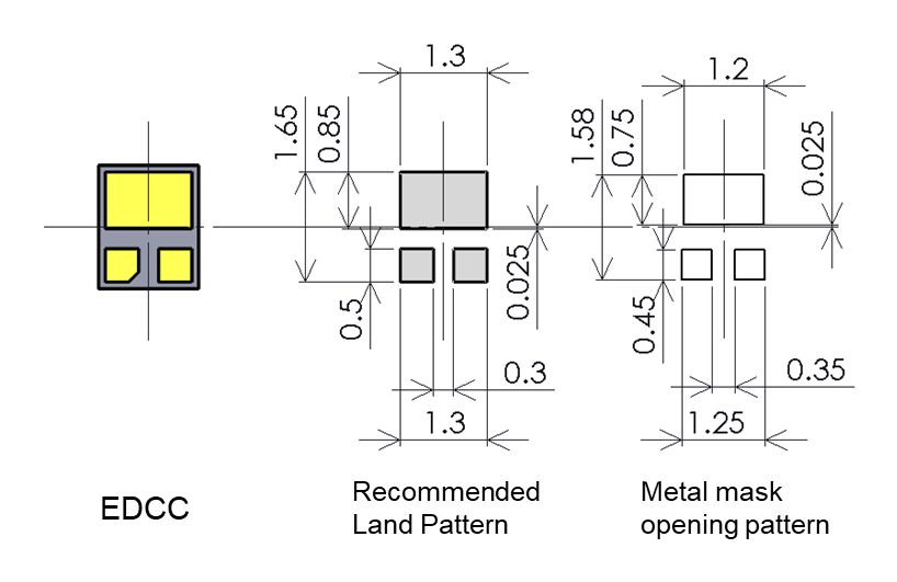
Recommended Land Pattern/Metal Mask Aperture Pattern
Release Date
| Category | Range | Release Date |
|---|---|---|
| UV | 365nm - 420nm | TBD |
| Visible | 430nm - 680nm | 2024 1Q |
| NIR | 690nm - 980nm | 2024 1Q |
| SWIR | 1050nm - 1900nm | 2024 1Q |
Single Junction Type
| Wavelength | Product Code |
|---|---|
| 470nm | EDCC470V-1100 |
| 525nm | EDCC525V-1100 |
| 590nm | EDCC590D-1100 |
| 670nm | EDCC670D-1100 |
| 700nm | EDCC700D-1100 |
| 720nm | EDCC720D-1100 |
| 740nm | EDCC740D-1100 |
| 760nm | EDCC760D-1100 |
| 780nm | EDCC780D-1100 |
| 810nm | EDCC810D-1100 |
| 830nm | EDCC830D-1100 |
| 850nm | EDCC850D-1100 |
| 880nm | EDCC880D-1100 |
| 890nm | EDCC890D-1100 |
| 940nm | EDCC940D-1100 |
| 970nm | EDCC970D-1100 |
| 1050nm | EDCC1050GD-1100 |
| 1070nm | EDCC1070D-1100 |
| 1100nm | EDCC1100D-1100 |
| 1150nm | EDCC1150D-1100 |
| 1200nm | EDCC1200D-1100 |
| 1300nm | EDCC1300D-1100 |
| 1370nm | EDCC1370D-1100 |
| 1450nm | EDCC1450D-1100 |
| 1550nm | EDCC1550D-1100 |
| 1650nm | EDCC1650D-1100 |
| 1900nm | EDCC1900D-1100 |
Dual Junction Series
| Wavelength | Model |
|---|---|
| 810nm | EDCC810DS-1100 |
| 850nm | EDCC850DS-1100 |
| 890nm | EDCC890DS-1100 |
| 940nm | EDCC940DS-1100 |
| 970nm | EDCC970DS-1100 |
For inquiries, please click here.
Loading...
Loading...
EDCC Series
The EDCC series is our revolutionary ultra-compact LED package offering chip-scale high-power performance. Measuring only 1.5 × 1.85 mm with a height of ~0.9 mm, EDCC LEDs are about 80% smaller than previous generation high-power packages. Despite their tiny size, they boast the highest power-to-size ratio in our lineup, capable of handling drive currents similar to larger LEDs. EDCC (which can be thought of as “Extreme Dynamic Chip-scale”) devices leverage advanced chip-scale packaging (CSP) techniques: the LED die is mounted with minimal packaging overhead, essentially approaching the footprint of the LED chip itself. The result is a powerful LED in a minuscule form factor that opens up new possibilities for wearable, portable, and densely arrayed LED applications.
Defining Features of EDCC LEDs
- Extreme Miniaturization (CSP Technology): EDCC LEDs are chip-scale package LEDs, meaning the package is not much larger than the LED die. With W ≈ 1.5 mm and L ≈ 1.85 mm, these devices are even smaller than standard 0603 components (which are ~1.6 × 0.8 mm). This incredible miniaturization is achieved through our innovative CSP design: there is no bulky housing; instead, the LED’s contacts and protective coatings essentially form the package. The EDCC series has been described as “extreme tiny CSP LED packages” heralding a new era of LED device design. When space is at an absolute premium, EDCC is the solution – they can fit in places that previously could only accommodate bare LED chips, yet they are easier to handle and solder like regular SMD components.
- High Power-to-Size Ratio: Even though EDCC LEDs are tiny, they are built to output serious light. They utilize high-efficiency LED chips (including flip-chip designs for many wavelengths) to maximize light emission. According to our internal benchmarks, an EDCC LED provides the highest luminous or radiant flux per unit area of any Tech-LED package. For example, an EDCC white or blue LED can produce brightness comparable to an older generation LED five times its size. In the IR range, we have EDCC IR LEDs (like 850 nm) that can easily handle 100 mA or more, yielding tens of milliwatts of IR power from a 1.5 mm device. This kind of performance previously required much larger LED packages with multiple chips.
- Wide Wavelength Range (UV to 1900 nm): Despite being chip-scale, EDCC is not limited in spectrum. We offer EDCC LEDs from UV 365 nm all the way to IR 1900 nm. This means you can get deep-UV LEDs in this ultra-compact form (useful for miniature UV sources in biomedical devices), as well as SWIR LEDs (for instance, 1350 nm or 1550 nm) in the same tiny footprint. The ability to cover 365–1900 nm in one package style is unprecedented. An EDCC LED thus could be chosen as the common building block for a multi-spectral array where each element is a different wavelength, simplifying the optics and assembly since all are identical in shape/size. The broad wavelength availability underscores Tech-LED’s strength in LED chip technology and packaging – very few manufacturers can deliver a 1.5 mm LED at, say, 1450 nm, but we do.
- Precision and Integration for Medical/Wearable Uses: The EDCC’s chip-scale nature allows it to be integrated into places previously impossible for LEDs. As noted in a recent Tech-LED insight, this technology “allows for integration into devices with limited space, enabling development of smaller, more discreet solutions”, particularly in fields like endoscopy and wearable monitoring. The key advantage here is that EDCC LEDs can be placed very close to other system components (sensors, optics, etc.), reducing optical path lengths and making very compact optical assemblies. They can even be integrated at the tip of medical instruments (like small catheters or needle-mounted scopes) where only a millimeter-scale component can fit. Additionally, multiple EDCC LEDs can be clustered to deliver higher intensity in a still-small area – akin to making a micro-LED array or “LED pixel”. Their small size and low weight also make them ideal for wearable devices, where any added weight or bulk is undesirable for user comfort.
- Customizable Array and Matrix Deployment: Because EDCC LEDs are so small and essentially flat, they can be arranged in high-density arrays or matrices for advanced lighting systems. Think of a scenario like a micro-LED display or a programmable illuminator: EDCC LEDs can be mounted with only ~0.2 mm gaps, creating a very fine pitch array. In fact, our research and development efforts have shown that EDCC packaging can facilitate micro-LED display tech (especially using UV EDCC chips with phosphor for micro-display pixels). We have a patent-pending structure that doubles the efficiency of micro UV-LED chips by special layer structuring, meaning EDCC isn’t just small – it’s also pushing efficiency boundaries at that scale. For customers, this means we can deliver micro-LED arrays that are brighter and more efficient than ever, in sizes suitable for AR/VR displays or very high-resolution lighting panels. Samples of such micro UV EDCC chips (~12 × 24 µm emitters) are available for cutting-edge display applications.
Breakthrough Applications for EDCC LEDs
The EDCC series truly shines in applications that were previously limited by LED size. A prime example is in medical devices, particularly invasive or wearable ones. As reported, EDCC LED packages are enabling a “new era in medical device design” by allowing lighting components to fit into unprecedentedly small tools. Consider a smart pill or implantable sensor: it might need an LED for illumination or signaling inside the body. With a conventional LED, even a 3 mm × 3 mm package might be too large or consume too much volume. An EDCC LED, being roughly half that size or less, makes it feasible to include light emission in ingestible devices or sub-cutaneous implants for short-term monitoring. Its chip-scale format minimizes the foreign material introduced, which is beneficial for biocompatibility as well.
Wearable health monitors can use EDCC LEDs for continuous measurement of vitals. For instance, an adhesive patch for measuring blood oxygen could integrate EDCC LEDs (say, red and IR) and photodiodes in a very thin form factor that sits on the skin like a bandage. Patients could wear it comfortably, and the high efficiency of EDCC ensures good signal quality even at low power. Similarly, earbuds or hearing aids with biometric functions might include EDCC heart-rate or oxygen sensors inside without changing their ergonomic shape, thanks to the minuscule LED size.
In augmented reality (AR) and virtual reality (VR), EDCC micro-LEDs are a game-changer for displays. AR systems are exploring micro-LED displays where tiny LEDs act as individual pixels to project images. Our EDCC technology, especially in UV with quantum-dot or phosphor conversion for full color, can be used to create ultra-fine pixelated light engines. The micro-LED chips on the order of 10–20 microns can be directly addressed on a CMOS backplane. Tech-LED’s micro UV-LED development (essentially applying EDCC concepts at even smaller scale) has achieved chips as small as 12 µm × 24 µm that maintain good efficiency. This opens the door for high-resolution, high-brightness AR displays in compact glasses, where traditional OLED or LCOS might fall short in brightness. The ability to produce and supply these micro-LEDs in volume is a cutting-edge application that Tech-LED is at the forefront of.
High-density lighting arrays are another domain. Imagine a studio light or automotive headlamp composed of thousands of tiny LEDs that can be individually controlled (for example, for adaptive driving beams or dynamic image projection). EDCC LEDs allow such arrays to be built with unprecedented LED count per area. An array of EDCC white LEDs could create a “pixelated” headlight that intelligently shapes the beam, or a programmable projector that’s all-solid-state. Because EDCC units are so small, the emitting surface can be filled almost completely with light sources, achieving very high luminance.
In summary, the EDCC series represents a breakthrough in LED packaging – delivering high-power optical output from a package nearly as small as the bare chip. This innovation is unlocking new applications in healthcare, wearables, AR/VR displays, miniaturized sensors, and adaptive lighting that were impractical with larger LEDs. By using EDCC LEDs, designers can create products that are lighter, smaller, and more discreet without sacrificing performance. Tech-LED’s EDCC is truly “reshaping the way we approach” LED integration in advanced technology, enabling minimally invasive procedures and highly portable devices that benefit patients and consumers alike. With wavelengths from 365 nm to 1900 nm available and record-breaking power density, EDCC is at the cutting edge of LED engineering – and we are ready to help customers incorporate this state-of-the-art solution into their next innovation.