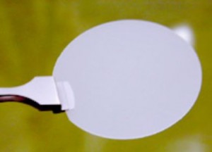
Epitaxial Wafers
This is the backbone technology expertise of advanced Solid-State Lighting as well as all photonics technologies. Marubeni-OPTO™ presents epitaxial wafers utilizing the latest in compound semiconductor crystalline growth technologies including Metal Organic Chemical Vapor Deposition (MOCVD). It is this critical growth process that builds up p- and n-crystal growth structures as well as p/n junction quantum wells that form the devices’ electron to photon conversion technology. Depending on the wafer and epitaxial process as well as various forms of crystalline doping techniques the wavelength for emission is established. Marubeni-OPTO™ specializes in “High-Brightness” LED technologies, offering a family of wafer epitaxial technologies stretching from the UV to Infrared wavelength emissions, including:
“The Nitrides” (AlInGaN):
This MOCVD technology area incorporates wafers that emit in the UV (heavily doped with Aluminum) to the visible Green wavelengths (heavily doped with Indium).


“The Phosphides” (AlInGaP):
This technology again utilizes MOCVD growth technology and runs from Yellow-Green to Red visible wafer products.
Aluminum Gallium Arsenide (AlGaAs):
This “High-Brightness” LED and sensor technology is the backbone for producing deep Red visible LEDs as well as Near Infrared through Mid-Infrared wavelengths (1550 nm, IR-B)
Marubeni-OPTO™ can supply your die fab ready epitaxial wafers, in standard formats or with custom varieties quoted upon request. We also offer laser-grade AlGaAs wafers.