
Short-wave infrared (SWIR) LEDs around 1200 nm represent a pivotal transition point between traditional infrared and the deeper SWIR region. This article explores what makes the 1200 nm wavelength special, how photodiode detectors behave at this crossover, and why engineers often choose LED emitters over lasers at 1200 nm. We delve into the semiconductor technology behind 1200nm LEDs, compare them to nearby IR wavelengths, and discuss high-power design challenges. Importantly, we highlight engineering applications – from semiconductor testing and materials inspection to optical characterization and short-range SWIR imaging – where 1200 nm LED sources provide unique advantages. Engineers, optical designers, and imaging system developers will find valuable information on leveraging 1200 nm light in practical systems.
For the broader SWIR LED context, how this wavelength fits within the 1050-1750 nm SWIR band, multispectral system design, and wavelength selection across the full SWIR range, see our SWIR LED Lighting Guide.
Why is 1200 nm LED light at the transition between infrared and SWIR?
The 1200 nm wavelength sits right at the boundary of what is traditionally considered near-infrared and the short-wave infrared (SWIR) band. In technical terms, silicon-based photodetectors – which dominate visible and near-IR sensing – have a bandgap corresponding to a cutoff around 1.1 μm (1100 nm). In fact, standard silicon photodiodes abruptly lose sensitivity beyond roughly 1.1 μm. This means light at 1200 nm is essentially invisible to normal silicon sensors, marking a clear dividing line between the IR that silicon can detect and longer SWIR wavelengths that require alternative detector materials. As a result, 1200 nm is often considered the crossover point from “IR” into “SWIR” in practical detector technology.
Notably, the transparency of silicon also changes at this boundary. Silicon becomes largely transparent to infrared light once wavelengths exceed about 1050 nm. For instance, a silicon wafer that is opaque under visible light will transmit most 1200 nm light. This transparency is one reason 1200 nm is useful – it allows infrared inspection through silicon substrates in ways not possible at shorter wavelengths. In summary, 1200 nm LED emission sits at a unique spot: it’s long enough in wavelength to pass through silicon (and thus behaves like SWIR), yet it’s just beyond the reach of conventional IR photodiodes. This crossover status defines its importance in optical engineering.
How do silicon and InGaAs photodiodes perform at 1200 nm?
The detector side of the equation highlights why the 1200 nm region is so critical. Silicon photodiodes – the workhorse detectors for up to ~1100 nm – rapidly lose responsivity as the wavelength approaches the silicon bandgap energy (~1.12 eV). Essentially, by 1200 nm a standard silicon photodiode has virtually zero quantum efficiency. Even advanced silicon-based solutions struggle here: for example, “black silicon” detectors with microstructured surfaces can extend detection slightly into the near-IR, but only efficiently up to about 1200 nm before responsivity plunges. This is a fundamental limitation of the semiconductor physics – photons with energy below the bandgap (like 1200 nm and longer for Si) cannot generate electron-hole pairs in silicon, or only do so via extremely inefficient processes.
To detect 1200 nm light and beyond, engineers turn to InGaAs (indium gallium arsenide) photodiodes and related lower-bandgap materials. InGaAs detectors pick up where silicon leaves off. A typical InGaAs photodiode is sensitive from roughly 900 nm up to about 1700 nm, covering the entire SWIR range. In fact, InGaAs sensor technology generally has peak responsivity around the 1300–1600 nm range, and still maintains significant sensitivity at 1200 nm. Thus, at the 1200 nm crossover, there is a detector technology hand-off: silicon devices stop being useful, and InGaAs-based detectors become the standard choice. This hand-off has practical implications – a 1200nm LED will typically be paired with an InGaAs photodiode or camera for detection, since a silicon photodiode or standard IR camera would miss most of that LED’s emission. The need for these specialized SWIR detectors also means higher cost and noise (InGaAs has higher dark current than Si due to its smaller bandgap), but it’s indispensable for capturing 1200 nm signals.
What detection challenges arise around the 1200 nm wavelength?
Operating right at the IR–SWIR boundary introduces some practical challenges for detection and system design. One issue is the “no man’s land” of detector responsivity around 1100–1200 nm – silicon is fading out, yet InGaAs is just coming into its prime. There can be a dip or gap in efficient detection if the wrong detector is used. Engineers must ensure their photodiode or camera is specified to cover ~1200 nm. Fortunately, most InGaAs sensors do cover this region, but the very edge cases (like some extended silicon or exotic detectors) might require calibration or special care. Additionally, the differing behavior of detectors means calibration standards change at 1200 nm. For example, optical power meters switch sensor types (from Si to thermal or InGaAs) when measuring beyond 1100 nm, to accurately capture the power output of a 1200 nm LED source.
Another challenge is the increased background and dark current in detectors that operate in the SWIR. InGaAs photodiodes have higher noise levels compared to silicon, especially if not cooled. At ~1200 nm, one can often use uncooled InGaAs sensors, but the signal-to-noise ratio may be lower than what a silicon detector would offer at shorter IR wavelengths. This means that applications at 1200 nm sometimes require stronger illumination or more averaging to achieve the same measurement precision. Nonetheless, advances in InGaAs sensor tech (like small-pixel high-sensitivity arrays) are continually improving the performance near this crossover, mitigating many of these concerns.
Why choose a 1200 nm LED emitter over an IR laser source?
When both LEDs and laser diodes can emit in the infrared, why would one opt for an LED at ~1200 nm? One key reason is the low coherence of LEDs, which translates to a major advantage: no laser speckle. Lasers produce coherent light that can create grainy interference patterns (speckle) on surfaces, complicating imaging and measurements. In contrast, an IR LED is an incoherent light source with a broad emission spectrum. This incoherence means when 1200 nm LED light illuminates a target, it produces a smooth, even illumination without the noisy speckle pattern that a laser of the same wavelength would generate. For imaging-system developers, reduced speckle leads to higher image quality and more reliable defect detection or measurement.
Another benefit of LEDs is their inherently broader beam and safer output for short-range use. A 1200nm LED typically emits over a wide angle (often 60° or more from a flat window package), rather than the narrow, intense beam of a laser. This makes LEDs easier to use for flood illumination of a scene at close range – no complex beam diffusers or moving optics are required to cover the field of view. The output power of an LED, while lower than a laser, is spread out and often in the eye-safe regime for 1200 nm (especially since the human eye cannot see 1200 nm and the beam is not focused). Engineers value that an LED-based illuminator can often be driven at high current without the stringent safety classification that a high-power IR laser would need. Additionally, LEDs are simpler in terms of drive electronics (they are current-driven devices that don’t require optical feedback loops or precision temperature tuning of wavelength). They turn on instantly and are stable in wavelength with temperature changes (only a minor shift), whereas laser diodes can exhibit mode hops or significant wavelength drift. For short-range systems where stability, uniformity, and safety are priorities, a 1200nm LED is often the preferred solution over a laser.
What materials and designs are used in 1200 nm LED technology?
Generating light at 1200 nm requires semiconductor materials with a smaller bandgap than the AlGaAs or GaAs alloys used for typical IR LEDs (which cover 850–940 nm). The industry solution has been to use indium gallium arsenide phosphide (InGaAsP) alloys on an InP substrate, which can be tuned to emit at various SWIR wavelengths. A 1200 nm LED generally uses an InGaAsP active layer engineered with the right composition to yield that emission peak. These materials are part of the same family used in telecom laser diodes at 1310 nm and 1550 nm, but in LED form they are designed for spontaneous emission rather than lasing. The LED die might be built as a double heterostructure or multi-quantum-well structure optimized for electroluminescence at 1.2 μm. Because the photon energy at 1200 nm is much lower than in visible LEDs, the internal efficiency tends to be lower and non-radiative recombination more significant. This is one reason early SWIR LEDs had quite low output power and efficiency compared to their visible counterparts. However, continuous improvements in the epitaxial growth and device design have boosted output in recent years.
In terms of packaging, 1200nm LEDs are available in similar form factors to other high-power infrared emitters. You can find them in standard through-hole packages (like T-1 3/4 epoxy-encased LEDs) which might output a couple of milliwatts, or in metal can packages with lens caps (TO-18 cans) that improve extraction efficiency and allow higher drive currents. For instance, one common design uses a TO-18 can with a built-in glass lens, yielding on the order of 5 mW output at 1200 nm. Surface-mount device (SMD) LEDs are also offered for SWIR wavelengths, enabling integration onto printed circuit boards like any SMD LED unit. These often feature flat window encapsulation or tiny lens caps. In all cases, current control is critical – as with any LED, a constant-current driver or appropriate series resistor is needed to regulate the LED’s forward current and prevent thermal runaway. Driving a 1200nm LED at high power (hundreds of mA) in a small package demands good heat sinking, because these devices do generate significant heat due to lower efficiency.
Optical design for 1200 nm LEDs often involves managing the emission angle and collection of light. Many SWIR LED packages come with either a flat window (emitting a wide Lambertian pattern, typically ±60° half-angle) or built-in lens optics to narrow the beam. For example, an LED with a flat encapsulation might cover a broad area, while variants with dome lenses can produce a ±10° or ±30° output beam for higher intensity in a smaller spot. Engineers choose the package type based on application – a wide-angle LED might illuminate an entire inspection area uniformly, whereas a narrow-angle LED can inject more power into a fiber optic or reach a distant target with higher intensity. In cases where even more power is required, manufacturers have developed multi-chip LED emitters. These combine multiple 1200 nm LED chips in one package or on one substrate (sometimes called LED arrays or clusters) to boost the total output. By driving, say, 4 or 8 LED chips in parallel within one emitter module, outputs in the tens or hundreds of milliwatts can be achieved while still maintaining low coherence output. Such high-power 1200nm LED assemblies make it feasible to use LED illumination for applications that previously might have needed a laser, all while retaining the LED advantages of simplicity and speckle-free light.
How does a 1200 nm LED compare to 1050 nm, 1300 nm, 1450 nm, and 1550 nm sources?
The infrared spectrum offers a continuum of LED and laser source options, and 1200 nm sits roughly in the middle of the short-wave IR choices. Compared to a 1050 nm IR LED, a 1200 nm LED will typically have slightly lower optical output for the same drive current. This is because as wavelength increases (photon energy decreases), it becomes harder to achieve high internal efficiency. A 1050nm LED can sometimes be built on a GaAs-based material system and may still be detectable by some silicon-based night-vision sensors, whereas at 1200 nm the LED must use the InP-based material system and absolutely requires an InGaAs detector. In terms of contrast, 1050 nm is near the edge of silicon’s range, so an imaging system at 1050 nm might get a weak signal on a silicon camera; but by 1200 nm, one has effectively zero crosstalk into silicon, which can be an advantage for avoiding interference with silicon-based sensors (for example, you could operate a 1200 nm targeting system alongside silicon CCTV cameras without the LED appearing on those cameras).
Looking toward longer wavelengths, 1300 nm and 1550 nm are famous as telecommunications bands – and indeed LEDs at those wavelengths exist (in fact, early fiber optic links often used 1300 nm LED transmitters). A 1300 nm LED will be quite similar in construction to a 1200 nm LED (using InGaAsP on InP). However, as the wavelength increases further to 1450 nm or 1550 nm, the challenges deepen. The LED’s efficiency drops and the output power for a single chip tends to be lower. For instance, a typical 1550 nm LED might only produce a few milliwatts unless multiple chips are combined. On the other hand, these longer wavelengths have some specific advantages in niche uses: 1550 nm is often considered “eye-safe” for lasers because the human eye’s lens and cornea absorb much of it, and 1450 nm corresponds to a strong water absorption line useful for moisture sensing. So while a 1200 nm LED is a good general-purpose SWIR illuminator, a 1450 nm LED might be chosen explicitly for detecting water content (where it strongly absorbs), and a 1550 nm LED might be deployed when maximum stealth or eye safety is needed, albeit typically in short-range scenarios due to limited LED power.
It’s worth noting that the range of SWIR LEDs has expanded in recent years. Specialized LED suppliers now offer a variety of wavelengths covering roughly 1050 nm up to 1650 nm or even 1750 nm. Thus, engineers can select an LED source tuned to the particular absorption feature or spectral window of interest. The 1200 nm LED stands out as the crossover point in this lineup – providing a balance of still moderate efficiency and the ability to reach beyond silicon’s limit. In comparison, a 1300 nm or 1550 nm LED may have lower radiant output but can interact with materials (like certain plastics or chemical overtones) that 1200 nm cannot. For example, some plastic resins have distinct absorption bands near 1200 nm and again near 1700 nm. If one’s inspection needs align with the 1200 nm absorption feature, a 1200 nm LED will be ideal; if not, a different SWIR LED in that “lineup” might be chosen. In summary, 1200 nm LEDs compare favorably as a middle-ground: easier to drive and brighter than the deepest SWIR LEDs, while reaching a part of the spectrum that 1050 nm sources can’t fully cover.
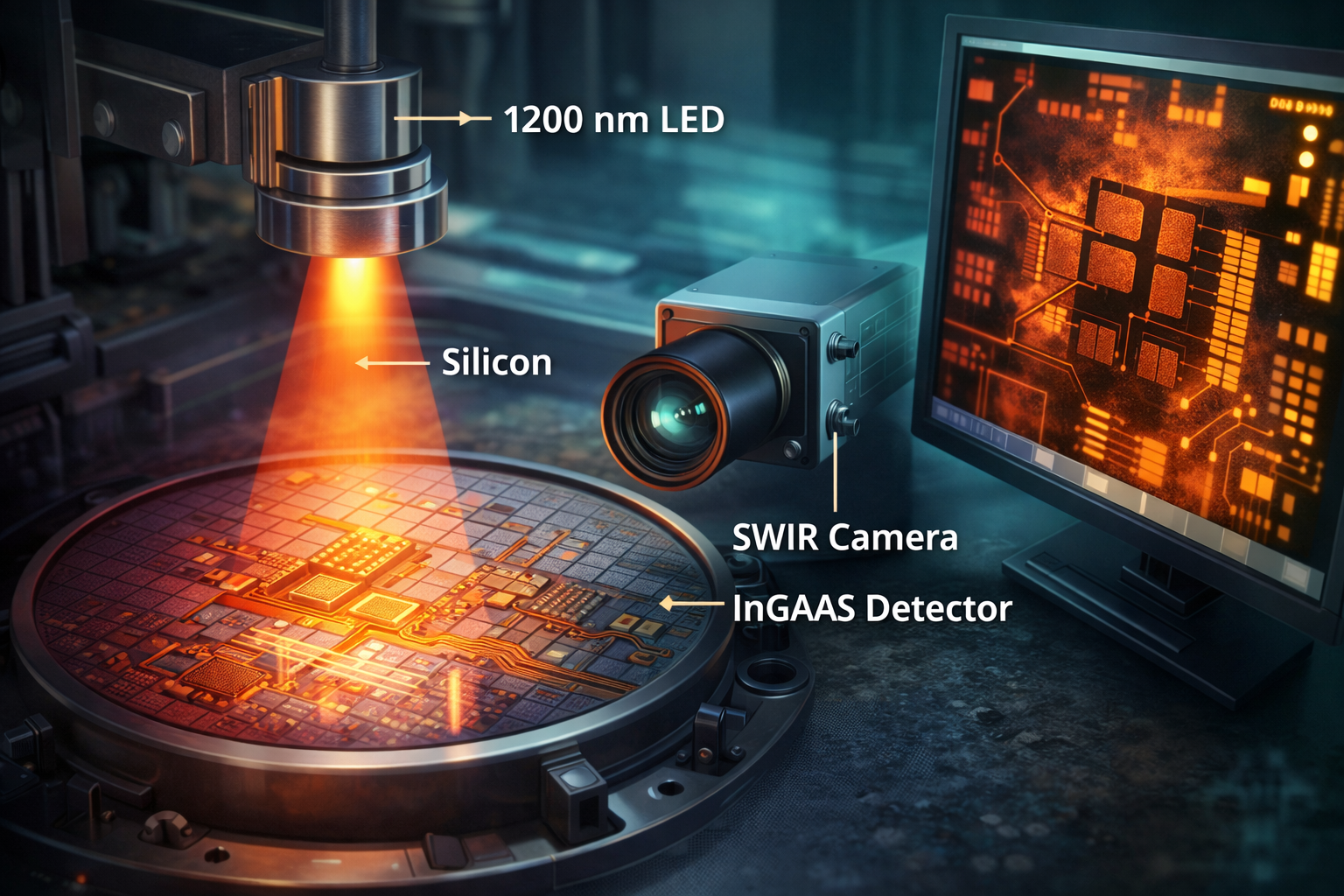
How are 1200 nm LEDs used in semiconductor testing and inspection?
One of the prime applications of 1200 nm LED sources is in semiconductor testing and inspection, particularly for silicon integrated circuits and wafers. Since silicon is nearly opaque to visible and most near-IR light, traditional optical inspection of a silicon wafer’s subsurface is impossible with visible illumination. However, at wavelengths around or above 1100 nm, silicon suddenly becomes transparent. By 1200 nm, a standard silicon wafer allows IR light to pass through relatively easily. This property is exploited in semiconductor failure analysis and wafer inspection: by illuminating a chip from the backside or through the wafer with 1200 nm infrared light, inspectors can image internal features like circuitry patterns, alignment marks, or defects that lie beneath the surface. SWIR cameras with InGaAs sensors can capture these transmitted or reflected IR images, revealing cracks, voids, or contamination inside the silicon that would be hidden at shorter wavelengths.
Because 1200 nm LEDs are high-power and incoherent, they make excellent illumination sources for such inspection systems. For instance, a ring of 1200 nm LED emitters can flood a wafer with uniform IR light during automated optical inspection. Any micro-cracks in silicon or subsurface structural anomalies will modulate the transmitted light and be picked up by the SWIR camera. Compared to a laser, the LED approach is safer for operators (no risk of a high-intensity laser beam) and provides even lighting with no speckle, improving the signal-to-noise for detecting small defects. In semiconductor testing labs, 1200 nm LED “IR illumination units” are often paired with zoom microscopes or infrared cameras to look at bonded wafer stacks, through-silicon vias, or die attach quality. The wavelength is a sweet spot: shorter IR like 1050 nm might not penetrate thicker silicon, whereas much longer like 1550 nm, while it penetrates, would require more expensive cameras and yields lower LED power. Thus, 1200 nm is a practical choice for silicon inspection needs, enabling non-destructive testing of silicon devices where visible light simply cannot reach.
How can 1200 nm infrared light aid in materials inspection and optical characterization?
Beyond semiconductors, 1200 nm LEDs find use in a variety of materials inspection roles. In industrial settings, one important application is moisture and chemical analysis. Many organic materials have specific absorption features in the SWIR range; for example, water has an absorption band near 1450 nm, but also smaller overtone absorption around 1200 nm. In agricultural or food product inspection, SWIR cameras often use a two-LED setup: one 1200 nm LED and one 1450 nm LED, pulsing alternately. At 1200 nm (outside the strong water band), the camera sees a reference image of the product, while at 1450 nm (inside the water absorption band) water-rich areas appear darker. By comparing the two, the system can map moisture content in grains, fruits, or packaged goods. The inclusion of 1200 nm as a baseline is crucial – it provides the “dry” reference reflectance. Similarly, 1200 nm light is absorbed by certain organic bonds (like C–H overtones), so it can help detect composition differences. For instance, some plastics or pharmaceutical tablets might reflect 1200 nm differently depending on polymer type or filler content, aiding sorting and quality control. Indeed, in recycling facilities, SWIR LED arrays (including 1200 nm emitters) combined with InGaAs line-scan cameras can differentiate plastic types on a conveyor, because common polymers have characteristic spectral fingerprints around 1200 nm and 1700 nm.
In optical instrumentation and characterization, 1200 nm LEDs serve as convenient light sources for various purposes. They can act as a stable, broad-spectrum source for calibrating spectrometers or testing optical filters meant for the SWIR range. For example, a researcher might use a 1200 nm LED to illuminate an optical fiber or an interferometer when characterizing system response in the IR-B band (approximately 1000–1400 nm). Unlike a thermal lamp, the LED provides a narrow-band output (with a typical spectral width of 25–50 nm) without the need for a monochromator, and unlike a laser, it won’t introduce coherent interference effects. This makes it easier to measure the insertion loss or spectral transmission of SWIR optical components – essentially the LED provides a known, smooth illumination profile. Additionally, because 1200 nm LEDs can be rapidly modulated (turned on/off at high frequencies), they are useful in time-resolved measurements and sensor calibration. For instance, an optical scientist might modulate a 1200 nm LED and use it to determine the speed response of a photodiode or to simulate pulsed signals in a fiber system. The LED’s emission is also relatively stable over time, so it can function as a reference source of information in an optical setup (for alignment or baseline signals).
In summary, whether it’s revealing moisture variation in materials, sorting products by composition, or serving as a benign test source in an optics lab, the 1200 nm infrared LED is a flexible tool. Its ability to interact with materials (via absorption/reflectance differences) and integrate into measurement systems without complications (no speckle, simple drive requirements) leads to a variety of applications in material inspection and optical characterization that benefit from this particular wavelength.
Why are 1200 nm LEDs ideal for short-range SWIR imaging?
Short-range imaging systems – such as machine vision cameras, security cameras, or handheld inspection devices – often require an active illumination source in the infrared. 1200 nm LEDs are well suited to these applications for several reasons. First, as mentioned earlier, the light is invisible to the human eye (and even to common night-vision goggles, which typically only see up to ~900 nm). This means an LED illuminator at 1200 nm can operate covertly or at least without visible distraction, while a SWIR camera captures the scene. For security or defense-related night vision, using an LED in the SWIR band allows observation of a scene with a SWIR sensor, but an observer with only standard IR imaging (or the naked eye) would see darkness. In essence, it’s an illumination invisible to most detection except dedicated SWIR cameras – a property highly valued in covert surveillance. In fact, 1200 nm is on the lower end of SWIR, so it balances covertness with slightly better atmospheric transmission than longer wavelengths. (At 1550 nm, one gets maximum stealth but more water absorption in air; at 1200 nm, propagation through air and common optics is a bit easier.)
Secondly, for short distances (from tens of centimeters to a few meters), one doesn’t need the long reach of a laser – instead, a broad LED flood works perfectly. High-power 1200 nm LED arrays can illuminate a wide area at short range with uniform intensity. This is ideal for machine vision on production lines (where SWIR cameras might inspect objects for certain features), since the LED can be mounted just a few inches away and angled to avoid glare. The lack of speckle and the stable output of LED light lead to clearer imaging of fine details like surface defects or fill levels behind translucent packaging. SWIR imaging excels at seeing through certain materials (for example, a SWIR light at 1200–1300 nm can sometimes see through a plastic container to view its contents, or through fabric to detect concealed objects, since many fabrics are more transparent in SWIR). Using an LED as the light source for these tasks ensures the illumination is safe (no laser hazard), diffuse, and easily synchronized with camera exposure. LEDs can be pulsed in microseconds, allowing high-speed gating or freeze-motion illumination without motion blur.
Finally, from a systems engineering perspective, LEDs are compact and rugged solid-state devices – this makes 1200 nm LED modules attractive for portable or harsh-environment SWIR imaging. There are no fragile bulbs or laser cavity alignments to worry about; an LED emitter can be packaged to be shock and vibration resistant, and it will typically last for tens of thousands of hours of operation. For short-range SWIR cameras (such as those used in field spectroscopy units, compact night vision scopes, or UAV-mounted inspection cameras), having a built-in 1200 nm LED illuminator is a robust solution. It provides a high-power SWIR light source in a small form factor and can be battery-powered with relatively low current draw compared to equivalent luminance from a lamp. All these reasons underscore why 1200 nm LEDs are a key enabling technology for short-range SWIR imaging systems – they offer a blend of performance, safety, and practicality that aligns perfectly with the needs of close-distance infrared observation.
- 1200 nm defines the IR–SWIR boundary: It’s the wavelength where silicon photodiodes stop working (cutoff ~1.1 μm), requiring InGaAs detectors and marking the transition into true SWIR.
- Silicon vs InGaAs detection: Silicon is blind at 1200 nm, whereas InGaAs photodiodes are highly sensitive in the 900–1700 nm range, enabling 1200 nm LEDs to be used in applications like through-silicon imaging and SWIR cameras.
- LEDs over lasers at 1200 nm: LED emitters provide low-coherence, speckle-free infrared light with a broad illumination angle – ideal for uniform short-range illumination without the interference artifacts or safety concerns of lasers.
- Specialized LED technology: 1200 nm LEDs use InGaAsP/InP semiconductor technology and come in packages from SMD LEDs to multi-chip high-power modules. They typically output a few to tens of milliwatts, with recent designs pushing into the 100+ mW range via multi-die arrays.
- Key engineering applications: 1200 nm LED sources enable semiconductor wafer inspection by transmitting IR light through silicon, materials sensing like moisture detection using 1200/1450 nm comparisons, optical spectroscopy and component testing in SWIR, and short-range SWIR imaging for machine vision or covert surveillance.
Putting 1200 nm in Context
This article fits within our broader wavelength-based framework for selecting infrared light sources across optical and imaging systems, anchored by our LED Wavelength Guide from UV to Infrared. While 1200 nm LEDs mark a clear transition into true SWIR, where silicon detectors give way to InGaAs, engineers often evaluate them alongside nearby wavelengths such as 1050 nm LEDs, which sit at the NIR–SWIR boundary, and longer-wavelength SWIR sources around 1300–1550 nm used for deeper penetration or eye-safe systems. Understanding how these adjacent wavelengths differ in detector compatibility, material interaction, and illumination behavior helps designers select the most effective infrared LED solution for semiconductor inspection, materials analysis, and short-range SWIR imaging.


